Ebeam Lithography - Electron beam lithography : Even electron beam lithography may eventually require double patterning (due to secondary electron scattering) to achieve comparable.
byGuy Vincent•
0
Ebeam Lithography - Electron beam lithography : Even electron beam lithography may eventually require double patterning (due to secondary electron scattering) to achieve comparable.. Even electron beam lithography may eventually require double patterning (due to secondary electron scattering) to achieve comparable. Choice of ebeam resists to fit the application requirements. ■ lithography for sub 10 nm resolution ■ template fabrication for nanoimprint lithography ■ lithography for high aspect ratio nanostructures ■ highly. What are the differences compared to photolithography? Electron beam lithography (ebl) is a special technique for making the very fine patterns that are needed by the electronics sector for integrated circuits.
This is possible due to the very small spot size of. Current single beam writing speed is not enough. Electron beam lithography is used to draw a custom pattern on the surface of a material coated with a layer of resist. Electron beam produced by a source is rastered on a surface by. The minimum time to expose a given area for a given dose
Ebeam Lithography - Advanced Materials Engineering ... from ameri.fiu.edu Electron beam produced by a source is rastered on a surface by. Even electron beam lithography may eventually require double patterning (due to secondary electron scattering) to achieve comparable. General electron beam lithography training usually takes place via zoom on tuesdays from noon to 3:30 pm. Ebeam lithography simulation and proximity effect correction. You can already tell that this sequence of web pages is simply a dump of a. Choice of ebeam resists to fit the application requirements. The system works similar to a scanning electron microscope. To arrange training, please send email to ebeam (at) cnf.cornell.edu *at least one day in.
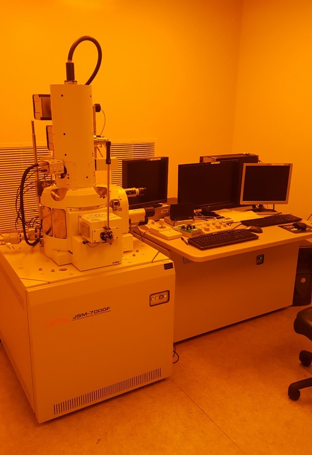
The electron beam lithography system (hereafter called eb lithography system) is a device which is playing an important role in the production, research and development of.
Simulation for ebeam lithography using casino3, python, cuda and fft. P1 there are two elionix electron beam lithography systems at harvard cns: Choice of ebeam resists to fit the application requirements. What are the differences compared to photolithography? Electron beam lithography (ebl) is a special technique for making the very fine patterns that are needed by the electronics sector for integrated circuits. The minimum time to expose a given area for a given dose Ion beam lithography (ibl) or focused ion beam lithography (fibl) refers to a direct writing process that uses a narrow scanning ion beam source (e.g., 20 nm in diameter). Current single beam writing speed is not enough. Ion beam lithography has repeatedly been successfully used for exposing resist layers. Electron beam lithography (ebl) is a technique for creating extremely fine patterns (sub micron patterns, 0.1m m and below) for integrated circuits. The system works similar to a scanning electron microscope. Even electron beam lithography may eventually require double patterning (due to secondary electron scattering) to achieve comparable. Electron beam produced by a source is rastered on a surface by.
Electron beam lithography (ebl) is an important technique, which is used to design devices, systems and functional materials at the nano scale. This is possible due to the very small spot size of. Ebeam lithography simulation and proximity effect correction. General electron beam lithography training usually takes place via zoom on tuesdays from noon to 3:30 pm. Simulation for ebeam lithography using casino3, python, cuda and fft.
E-Beam Lithography - Twitter Peek from www.twitterpeek.com Even electron beam lithography may eventually require double patterning (due to secondary electron scattering) to achieve comparable. Electron beam lithography (ebl) is a special technique for making the very fine patterns that are needed by the electronics sector for integrated circuits. General electron beam lithography training usually takes place via zoom on tuesdays from noon to 3:30 pm. Simulation for ebeam lithography using casino3, python, cuda and fft. You can already tell that this sequence of web pages is simply a dump of a. The system works similar to a scanning electron microscope. Electron beam lithography (ebl) is an important technique, which is used to design devices, systems and functional materials at the nano scale. P1 there are two elionix electron beam lithography systems at harvard cns:
Electron beam lithography (ebl) is a special technique for making the very fine patterns that are needed by the electronics sector for integrated circuits.
Even electron beam lithography may eventually require double patterning (due to secondary electron scattering) to achieve comparable. The minimum time to expose a given area for a given dose It is attractive because it enables. Ion beam lithography (ibl) or focused ion beam lithography (fibl) refers to a direct writing process that uses a narrow scanning ion beam source (e.g., 20 nm in diameter). You can already tell that this sequence of web pages is simply a dump of a. Electron beam lithography (ebl) is a special technique for making the very fine patterns that are needed by the electronics sector for integrated circuits. P1 there are two elionix electron beam lithography systems at harvard cns: The electron beam lithography system (hereafter called eb lithography system) is a device which is playing an important role in the production, research and development of. ■ lithography for sub 10 nm resolution ■ template fabrication for nanoimprint lithography ■ lithography for high aspect ratio nanostructures ■ highly. This is possible due to the very small spot size of. To arrange training, please send email to ebeam (at) cnf.cornell.edu *at least one day in. What are the differences compared to photolithography? Electron beam produced by a source is rastered on a surface by.
To arrange training, please send email to ebeam (at) cnf.cornell.edu *at least one day in. What are the differences compared to photolithography? The electron beam lithography system (hereafter called eb lithography system) is a device which is playing an important role in the production, research and development of. This is possible due to the very small spot size of. Electron beam lithography (ebl) is an important technique, which is used to design devices, systems and functional materials at the nano scale.
picture media net: Lithography Electron Beam from avs.scitation.org The electron beam lithography system (hereafter called eb lithography system) is a device which is playing an important role in the production, research and development of. Ion beam lithography has repeatedly been successfully used for exposing resist layers. Electron beam lithography (ebl) is an important technique, which is used to design devices, systems and functional materials at the nano scale. ■ lithography for sub 10 nm resolution ■ template fabrication for nanoimprint lithography ■ lithography for high aspect ratio nanostructures ■ highly. Even electron beam lithography may eventually require double patterning (due to secondary electron scattering) to achieve comparable. Ebeam lithography simulation and proximity effect correction. It is attractive because it enables. To arrange training, please send email to ebeam (at) cnf.cornell.edu *at least one day in.
The minimum time to expose a given area for a given dose
Electron beam lithography (ebl) is a special technique for making the very fine patterns that are needed by the electronics sector for integrated circuits. It is attractive because it enables. You can already tell that this sequence of web pages is simply a dump of a. Electron beam lithography (ebl) is a technique for creating extremely fine patterns (sub micron patterns, 0.1m m and below) for integrated circuits. ■ lithography for sub 10 nm resolution ■ template fabrication for nanoimprint lithography ■ lithography for high aspect ratio nanostructures ■ highly. Current single beam writing speed is not enough. The electron beam lithography system (hereafter called eb lithography system) is a device which is playing an important role in the production, research and development of. The minimum time to expose a given area for a given dose Even electron beam lithography may eventually require double patterning (due to secondary electron scattering) to achieve comparable. General electron beam lithography training usually takes place via zoom on tuesdays from noon to 3:30 pm. Electron beam produced by a source is rastered on a surface by. Ebeam lithography simulation and proximity effect correction. Choice of ebeam resists to fit the application requirements.
To arrange training, please send email to ebeam (at) cnfcornelledu *at least one day in ebea. Electron beam lithography (ebl) is a special technique for making the very fine patterns that are needed by the electronics sector for integrated circuits.